Design a Lag Compensator Using Frequency Domain Methods
6.3: Frequency Response Design
-
- Last updated
- Save as PDF
- Page ID
- 24415
The frequency response design involves adding a compensator to the feedback loop to shape the frequency response function. The design aims to achieve the following:
- A desired degree of relative stability and indicated by the phase margin.
- A desired speed of response as indicated by the gain crossover frequency.
- A mild slope of \(-1\) (or \(-20dB/\rm decade)\) at the crossover.
The choice of compensators in the frequency response design method includes the gain compensator, the phase-lag and phase-lead compensators, and the PD, PI, and PID compensators. These are described next.
Gain Compensation
The gain compensation aims to add a static compensator, \(K(s)=K\), to the feedback loop.
The gain compensation raises the loop gain by \(K\); the Bode magnitude plot is shifted up by \(20\; \log _{{\rm 1}0} \; K.\) The resulting change in the gain crossover frequency, \(\omega _{{\rm g}c}\), affects the \({\rm PM}\).
The phase margin is reduced for (\(K>1\)), and increased for (\(K<1\)). Further, the system bandwidth increases for (\(K>1\)), which improves the transient response by reducing the settling time. This is illustrated in the following example.
Example \(\PageIndex{1}\)
Let \(G(s)=\frac{2}{s(s+1)(s+2)}\); assume that the performance specifications state a \(50{}^\circ\)phae margin.
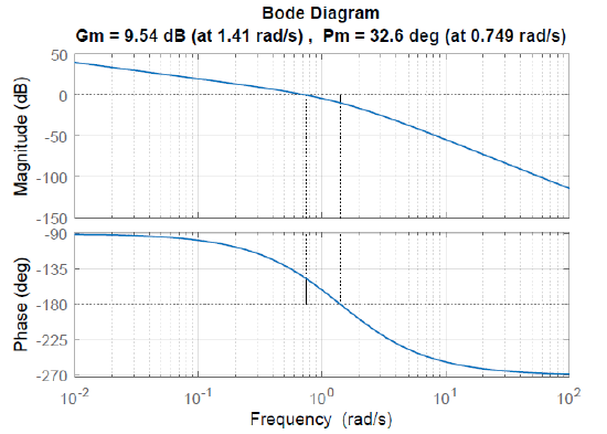
For \(K=1\), the GM, PM and the crossover frequencies are obtained from MATLAB as: \({\rm GM}=3\; (9.54\; {\rm dB}),\; \; \omega _{\rm pc} =1.41\;\frac{\rm rad}{\rm s} ;\; \rm PM=32.6^{\circ } ,\; \; \omega _{\rm gc} =0.749\; \frac{\rm rad}{\rm s}\).
The gain crossover frequency need to be reduced to increase the phase margin. We observe from the Bode plot that \(|G(j0.49)|=5\; \rm dB\) and \(\phi \left(j0.49\right)=-130{}^\circ\).
Thus, reducing loop gain by \(5dB\) will affect a crossover at \({\omega }_{\rm gc}=0.49\; \frac{\rm rad}{\rm s} \) and achieve a \(\rm PM=50^{\circ }\). The required gain compensator is given as: \(K=0.56\).
The design is verified by plotting the frequency response for the loop transfer function: \(KG(s)=\frac{1.12}{s(s+1)(s+2)}\), which shows \(PM=50^{\circ }\) at the new \(\omega _{\rm gc} =0.49\; \frac{\rm rad}{\rm s}\) (Figure 6.3.1).


Phase-Lag Compensation
In the frequency response design, the phase-lag compensator serves a dual purpose: it can improve the phase margin (a measure of transient response), as well the DC gain (a measure of steady-state response).
The phase-lag compensator is described as:
\[ K(s) =\frac{K(1+s/\omega _z )}{1+s/\omega _p } ,\;\; K(j\omega ) =\frac{K(1+j\omega /\omega _ z )}{(1+j\omega /\omega _ p )},\;\; \omega _z >\omega _p \]
Phase Margin Improvement. For \(K=1\), the phase-lag compensator is characterized by: \(\left|KG\left(j0\right)\right|=0dB\) and \(\left|KG\left(j\infty \right)\right|=-20{log \left(\frac{{\omega }_z}{{\omega }_p}\right)\ }\). Thus, the addition of the compensator to the feedback loop will lower the gain crossover frequency and increase the phase margin.
Error Constant Improvement. Alternatively, let \(K=\frac{{\omega }_z}{{\omega }_p}\); then, the phase-lag compensator is characterized by: \(KG\left(j0\right)=20{log \left(\frac{{\omega }_z}{{\omega }_p}\right)\ }\) and \(KG\left(j\infty \right)=0dB\). Since the DC gain of the compensator is greater than one, addition of the compensator to the feedback loop will boost the relevant error constant by a factor of \(K=\omega _{z} /\omega _{p} \).
In order to minimize the adverse phase contribution from the compensator, the compensator pole and zero locations for steady-state error improvement must be selected in accordance with: \(\omega _\rm p <\omega _\rm z <0.1\omega _{\rm gc}\), where \(\omega _{gc}\) is the gain crossover frequency.
Compensator Design. The phase-lag compensator design is summarized below:
- Use gain compensation to adjust the dc gain \(\left|KGH\left(j0\right)\right|\) to the desired value to meet the steady-state error requirement.
- On the Bode plot of \(KGH(j\omega )\), select a frequency \(\omega _{1}\) to satisfy \(\angle KGH(j\omega _{1} )=-180^{\circ } +\phi _\rm m +5^{\circ }\), where \(\phi _\rm m\) is the desired phase margin, \(\omega _{1}\) serves as the new gain crossover frequency, and \(5^{\circ }\) is a safety margin to compensate for an estimated: \(\angle K(j\omega _{1} )\cong -5^{\circ }\).
- Select the compensator pole and zero frequencies as: \(\omega _\rm z \; =\; 0.1\omega _{1} ,\; \omega _\rm p \; =\; \omega _\rm z /|KGH(j\omega _{1} )|\).
- Draw the Bode plot for the compensated system and verify the design.
Example \(\PageIndex{2}\)
Let \(G(s)=\frac{2}{s(s+1)(s+2)}\); assume that the design specifications are: \(PM=50^{\circ }\), and \(e_{ss} |_{\rm ramp} <0.1\)(\(K_v >10\)). Then, the phase-lag compensator proceeds as follows:
- Choose \(K=11\) to meet the error constant requirement.
- From the Bode plot for \(KG(j\omega )\); choose \(\omega _{1} =0.4\; {\rm r}ad/s\) for \(\angle KG(j\omega _{1} )=-123^{\circ }\); then, \(\left|{\rm K}G(j\omega _{1} )\right|=24.9\; (28\; \rm dB)\).
- Choose \(\omega _\rm z =0.04,\; \omega _\rm p =0.0016\); then, \(K(s)=\frac{11(1+s/0.04)}{1+s/0.0016}\).
- The Bode plot of the compensated system shows \(\omega _{{\rm g}c} =0.4\; {\rm r}ad/s\) and \(\rm PM=51^{\circ }\) (Fig. 6.3.2).


Phase-Lead Compensation
In the frequency response design, the phase-lead compensator serves to increase the closed-loop bandwidth, leading to transient response improvements. The phase-lead compensator is described by the transfer function:
\[K(s)=\frac{K(1+s/\omega _ z )}{1+s/\omega _ p } ,\; \, K(j\omega )=\frac{K(1+j\omega /\omega _ z )}{(1+j\omega /\omega _ p )} ,\; \; \omega _ z <\omega _ p\]
Bandwidth Improvement. For \(K=1\), phase-lead compensator response is characterized by: \(\left|KG\left(j0\right)\right|=0dB\) and \(\left|KG\left(j\infty \right)\right|=20{log \left(\frac{{\omega }_p}{{\omega }_z}\right)\ }\).
Since the high frequency gain of the compensator is greater than one, its addition to the feedback loop increases the crossover frequency and the bandwidth.
The compensator contributes maximum phase-lead \(\theta _m\) at a frequency \(\omega _ m =\sqrt{\omega _ z \omega _p }\).
To proceed further, let \(\alpha =\frac{\omega _ p }{\omega _ z }\); then, \(\sin \theta _ m \; =\frac{\alpha -1}{\alpha +1}\), or \(\alpha =\frac{1+\sin \theta _ m }{1-\sin \theta _ m \; }\). Further, the compensator pole and zero locations are obtained as: \(\omega _ z =\frac{\omega _ m }{\sqrt{\alpha } } ;\; \omega _ p =\omega _ m \sqrt{\alpha }\).
Practically, the maximum achievable value of \(\theta _ m\) is about \(70^{\circ }\) for \(\sqrt{\alpha }\cong 6\).
The compensator transfer function at \(\omega _ m\) is given as: \(K\left(j{\omega }_m\right)=K\sqrt{\alpha }\). Then, from the crossover condition: \(\left|KGH\left(j{\omega }_{gc}\right)\right|=1\), we obtain: \(K=\frac{\sqrt{\alpha }}{\left|GH\left(j{\omega }_{gc}\right)\right|}\).
Compensator Design. The phase-lead design involves the following steps:
- Choose a desired crossover frequency, \(\omega _{\rm gc}\), as the greater of \(\frac{8}{t_ s \tan \phi _ m \; }\) and \(\omega _{1}\) where \(\angle KGH(j\omega _{1} )=-180^{\circ } +\phi _\rm m +5^{\circ }\).
- Compute the required compensator phase angle: \(\theta =\phi _ m -\angle G(j\omega _{\rm gc} )-180^{\circ }\); compute \(|GH(j\omega _{\rm gc} )|.\)
- Solve for \(\omega _ z\) and \(\omega _ p\).
- Inspect the Bode plot of the compensated system and verify the design.
Example \(\PageIndex{3}\)
Let \(G(s)=\frac{2}{s(s+1)(s+2)}\); \(PM=32.6^{\circ }\). The design specifications are: \(\phi _ m =50^{\circ }\), \(t_ s =4\; \rm s\). Then, the phase-lead compensator design steps are:
- From the settling time requirement, we have, \(\omega _{\rm gc} =\frac{2}{\tan \phi _ m } =1.68\; \frac{\rm rad}\rm s ;\;\)then, \(\theta =50^{\circ } +9^{\circ } =59^{\circ } \cong 60^{\circ }\). Further, \(G(j1.68)=0.23\; \angle -189^{\circ } .\)
- For \(\theta =60{}^\circ\), we have \(\alpha =13.93\); the phase-lead design is given as:
\({\omega }_z=0.45\frac{\rm rad}{\rm s}\), \({\omega }_p=6.27\frac{\rm rad}{\rm s}\), \(K=16\); thus \(K\left(s\right)=16\left(\frac{s+0.45}{s+6.27}\right)\)
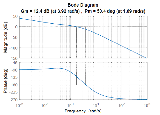
The Bode plot of the compensated system has \(\phi _{m} =50.4^{\circ }\) at \(\omega _{{\rm g}c} =1.69\; \frac{\rm rad}{\rm s}\) (Figure 6.3.3).


Lead-Lag Compensation
A lead-lag compensator combines the phase-lead and phase-lag sections. The phase-lag section improves the phase margin and the dc gain; the phase-lead section improves the bandwidth and the phase margin. Since both lead and lag sections can contribute to the phase margin improvement, the desired PM improvement can be distributed among the two sections.
The lead-lag compensator transfer function is given as: \(K(s)=K_{lead} (s)K_{lag} (s).\)
The steps to design a lead-lag compensator are as follows:
- Choose static gain \(K\) to meet the steady-state error requirement.
- Design the phase-lag section to meet part of the phase margin requirement.
- Design phase-lead section to meet the bandwidth/settling time requirement.
Example \(\PageIndex{4}\)
Let \(G(s)=\frac{2}{s(s+1)(s+2)}\); assume that the design specifications are: \(\phi _ m =50^{\circ }\), \(t_ s =4s\), and \(e_{\rm ss} |_{\rm ramp} \; <0.1\). The design steps for the lag-lead design are as follows:
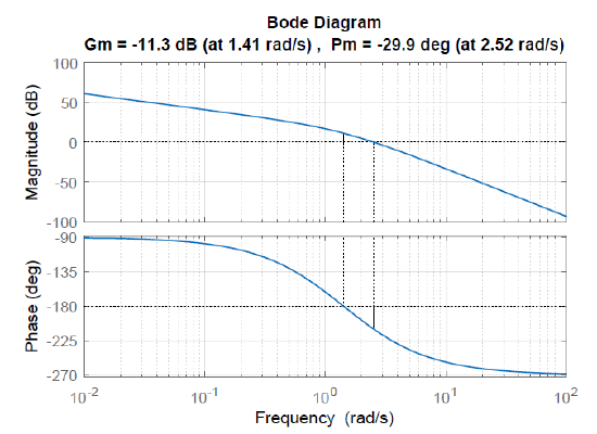
- DC Gain. Choose \(K=10\) to meet the \(e_{\rm ss}\) requirement. Draw the Bode plot for \(KG(s)\). The plot has \(\omega _{{\rm g}c} =2.5\; {\rm rad/s}\) and \(\rm PM=-30^{\circ }\).
- Phase-Lag Design. Suppose we aim to raise the phase margin to \(\rm PM\approx 40^{\circ }\). From the Bode plot, let \(\omega _{1} =0.5\; {\rm rad/s}\), such that \(KG\; (j0.5)=18.6\; (25.8\; \rm dB)\angle -130^{\circ }\).
- Complete the phase-lag design with: \(\omega _\rm z =0.05,\; \omega _\rm p =0.003.\)
- Phase-Lead Design. From the Bode plot of \(K_{lag} G(j\omega )\) choose \(\omega _{\rm gc} =1.7\; {\rm rad/s}\) to meet the \(t_s\) requirement. Then, \(K_{lag} G(j1.7)=0.15\; (-16.5\; \rm dB)\angle -191^{\circ } .\)
- Compute the phase-lead compensator parameters: \(\theta =62^{\circ }\), \(\alpha =16,\ K=26.7,\ {\omega }_z=0.425\ rad/s,\ {\omega }_p=6.8\ {\rm rad/s}\).
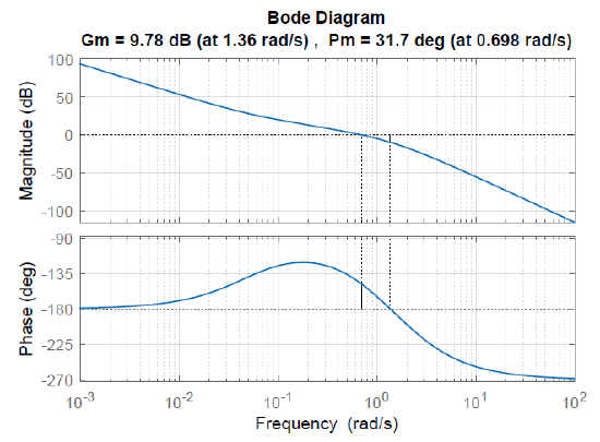
- The lead-lag compensator is described as: \(K(s)=\frac{11(s+0.05)(s+0.24)}{(s+0.003)(s+4.7)}\). The Bode plot for the compensated system has \(\rm PM=50.2^{\circ }\) at \(\omega =1.71\; {\rm rad/s}\) (Figure 6.3.4).


The PID Compensator
The PID compensator is a combination of the PI and PD sections. The PI compensator adds an integrator to the feedback loop that reduces the steady-state error to zero; the PI compensator can also realize the PM requirement. The PI compensator is defined as:
\[K(s)=k_{p} +\frac{k_{i} }{s} ,\;\; K(j\omega ) =\frac{k_{i} (1+j\omega /\omega _{z} )}{j\omega } ,\;\;\omega _{z} =\frac{k_{i} }{k_{p} }\]
The PI compensator zero is arbitrarily located close to the origin. The gain \(k_i\) is selected to achieve a desired PM improvement.
The PD compensator adds a first-order zero to the loop transfer function, which increases the bandwidth and hence the transient response. The PD compensator is defined as:
\[K(s)=k_{d} s+k_{p} ,\; K(j\omega )=k_{p} (1+j\omega /\omega _{z} )\]
The desired gain crossover \(\omega _{gc}\) is selected as the greater of \(\frac{8}{t_ s \tan \phi _ m }\) and \(\omega _{1}\), where \(\omega _{1}\) is found from the Bode plot for \(\angle KGH(j\omega _{1} )=-180^{\circ } +\phi _\rm m -90^{\circ } +5^{\circ } ;\) the \(90^{\circ }\) term in this expression refers to the phase added by the PD compensator, and \(5^{\circ }\) is a safety margin.
The compensator zero location may be selected as: \({\omega }_z=0.1{\omega }_{gc}\); the compensator gain \(k_p\) is selected to meet the crossover condition: \(|KGH(j\omega _{gc} )|=1\).
Example \(\PageIndex{5}\)
Let \(G(s)=\frac{2}{s(s+1)(s+2)}\); assume that the design specifications are: \(\phi _ m =50^{\circ }\), \(t_ s =4\; \rm s\), and \(e_{\rm ss} |_{\rm ramp} <0.1\).
No gain adjustment is needed as the PI compensator will boost the position error constant \(K_{\rm p}\to\infty\).
- PI design. We aim to achieve \(PM=30{}^\circ\) in the PI section. The Bode plot for \(G(j\omega )\) has \(G(j0.8)=0.9\; \angle -150^{\circ } .\) Let \(\omega _z =0.05\); then \(K_{PI} (s)=\frac{0.9(s+.05)}{s}\).
- PD design. From the settling time requirement, \(\omega _{\rm gc} =\frac{2}{\tan \phi _\rm m } \cong 1.7\; \frac{\rm rad}{\rm s} ;\;\) from the phase angle requirement, \(\omega _{1} =2.5\; \frac{\rm rad}{\rm s}\); hence, \(\omega _{\rm gc} =2.5\; \frac{\rm rad}{\rm s};\) the Bode plot of \(K_{PI} G(j\omega )\) shows \(G(j2.5)=0.1\; \angle -210^{\circ } .\)
- The PD compensator is zero selected as: \(\omega _ z =0.2\; \frac{\rm rad}{\rm s} ,\; K_{PD} (s)=5(s+0.2)\).
- The PID compensator is given as: \(K(s)=\frac{4.5(s+0.05)(s+0.2)}{s}.\) The Bode plot of the compensated system has \(\phi _ m =53.4^{\circ }\) at \(\omega _{\rm gc} =2.58\; \frac{\rm rad}{\rm s}\) (Figure 6.3.5).


Design a Lag Compensator Using Frequency Domain Methods
Source: https://eng.libretexts.org/Bookshelves/Industrial_and_Systems_Engineering/Book%3A_Introduction_to_Control_Systems_(Iqbal)/06%3A_Compensator_Design_with_Frequency_Response_Methods/6.03%3A_Frequency_Response_Design
0 Response to "Design a Lag Compensator Using Frequency Domain Methods"
Postar um comentário